

As a maker, I always wanted to create a PCB (printed circuit board) online but making PCBs always seemed like a tedious task. Then I came across a free online tool called EasyEDA. In this article, I will show you how to get started with EasyEDA to start creating professional PCBs for your projects.
For this project, I will walk you through the process of designing and manufacturing a PCB for an IR Proximity Sensor. Let’s get started!
Step 1: Planing the Custom PCB Design
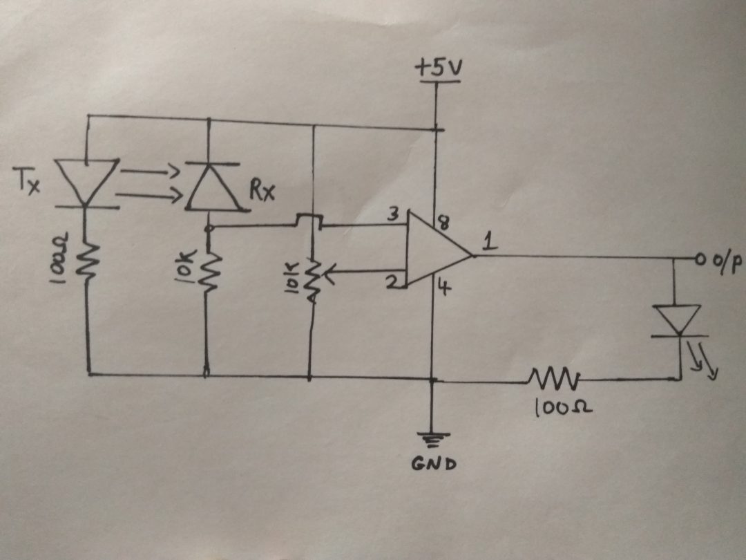
First, we need to plan the design by drawing a circuit diagram on paper. Once the diagram is complete, we can make a prototype on a breadboard to test out the circuit. Make adjustments to the circuit drawing as needed.
Now that we have a working circuit, we can finalize the design in software.
Step 2: Making a Circuit Online with EasyEDA
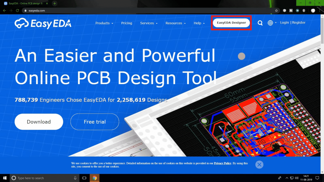
There are many online tools to make custom PCBs online. For this project, we will use EasyEDA. Here you can either download the tool or use the online designer. Then, click on the EasyEDA Designer to use the online tool.
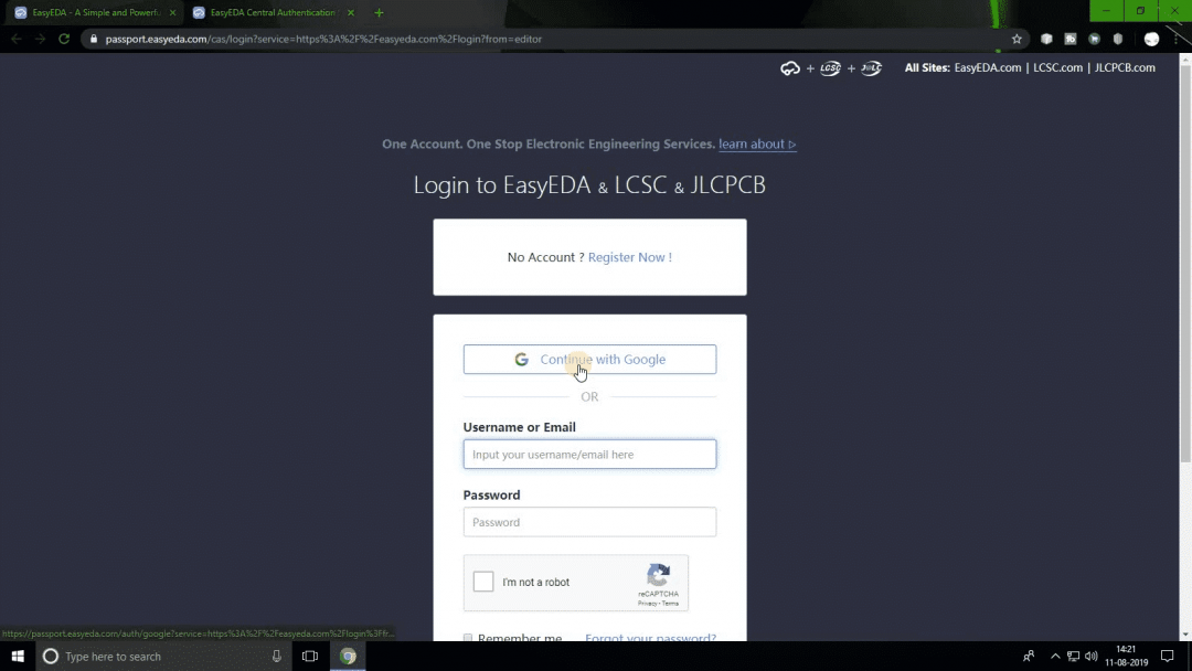
Now, we need to create an account with EasyEDA. Click on “Projects” and “Log in” from the left menu. Create an account or sign in.
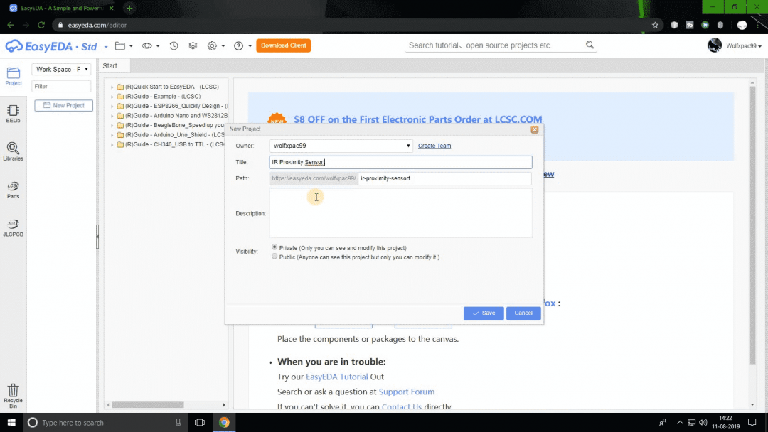
Next click on “New Project.” Give the project a name and description. I named the project “IR Proximity Sensor.”
Save the project. You’ll notice a blank canvas and some part symbols on the left side. We will use these parts to make our design. If you can’t find a part, you can look in the Libraries. Just search for the part you are looking for. Make sure it has a symbol and PCB footprints.
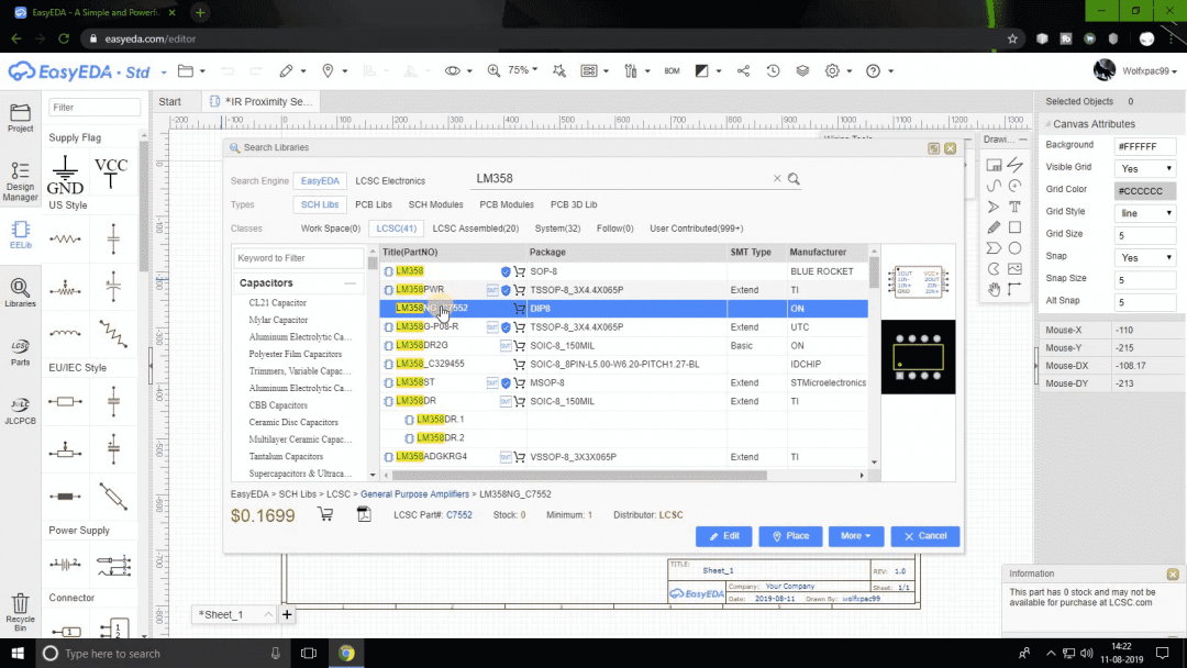
Double-click on the part to select it, and place it on the canvas. Then search for the next part. Repeat this process for the remaining parts. Use your hand-drawn circuit diagram to create a digital circuit. Draw the wires by clicking on the end of one part and the terminal of the other part.
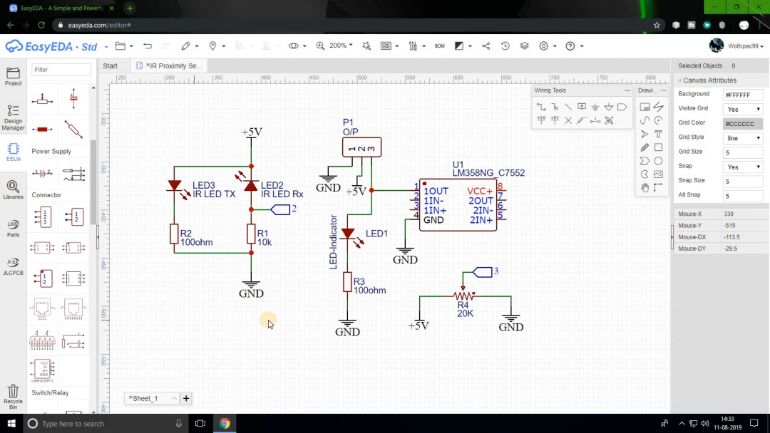
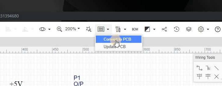
In the above diagram, the GND represents the ground connections and +5V represents the power connections. When you are happy with the design, convert this circuit into a PCB. To do this, first, click on the PCB option from the top menu (next to the star icon). Then select “Convert to PCB.”
Step 3: Make the PCB Design Online
EasyEDA might ask you to check the nets or connections, but you can skip this if you are sure your connections are correct. You will see a new tab with a border and components which you have to arrange on the board.
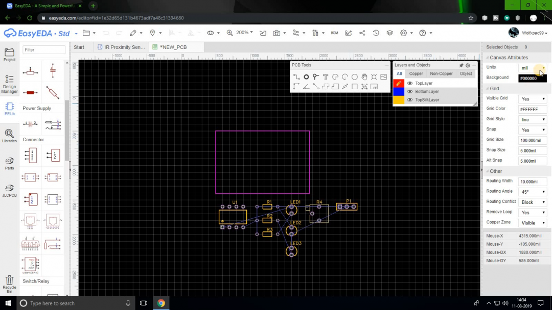
Start arranging the components on the board. Make sure you place those components physically closer which are connected directly. This will make routing easier and less complex. After placing all the components we can start routing.
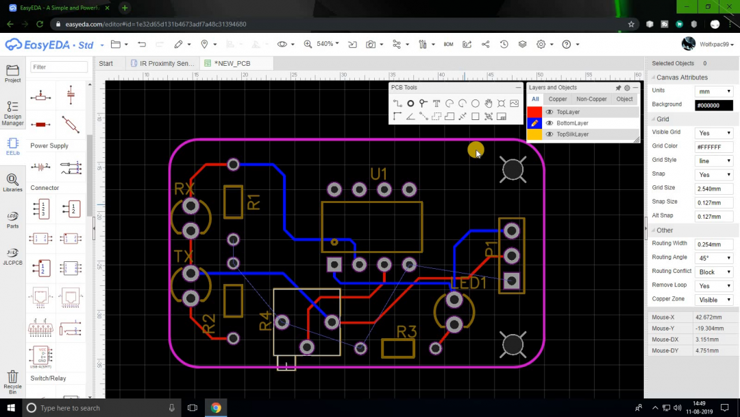
PCB Routing is when you add traces that will connect components. As a hobbyist, we will make 2-layer PCBs because they are more affordable to manufacture. The red traces represent the top layer and the blue traces represent the bottom layer. You can always add more layers, but they will increase the cost of your board.
How to Route PCB Traces
EasyEDA also has an Autorouter tool which will make the traces for you. This tool works great for small and less complex circuits but it might make errors in big projects. I recommend manual routing.
Here are some key things to consider when wiring traces on your PCB design.
- Use thicker tracks for power lines.
- Avoid 90° turns while making traces. Traces might get etched off easily at 90°. Also, it tends to cause a lot of noise in the circuit which may affect Wireless applications.
- Do not connect GND traces. Use the copper area tool at the end to create a single ground plate.
- Make sure you keep a good clearance between traces and ground plates to avoid any short circuits.
- Never make traces near the edge of the PCB or the screw holes.
Once you are happy with your traces, double-check the routes, and save the PCB file.
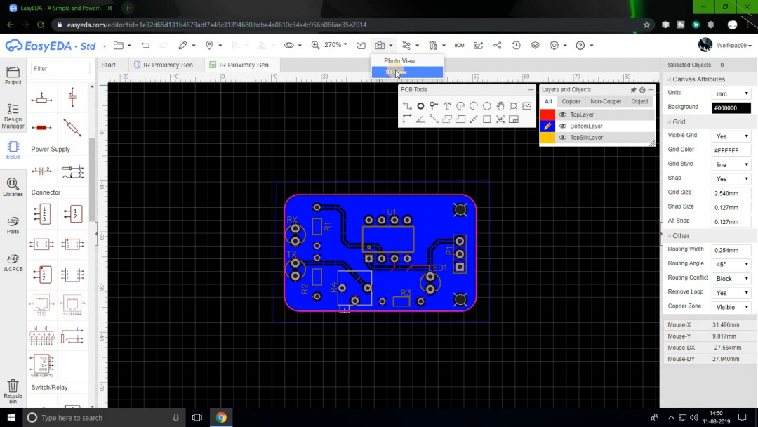
Step 4: 3D Preview and Gerber Files
You can see how the product will look after production before generating the PCB files (also known as Gerber files). Open the 3D viewer in EasyEDA by clicking on the camera icon in the top bar and selecting “3D viewer”.
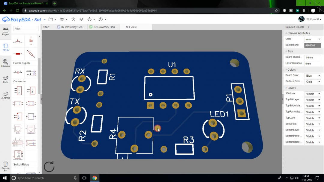
The 3D model will take a couple of seconds to load. Use this model to see how the final board will look. Once you’re satisfied with the look, go back to the PCB tab and click on the G icon.
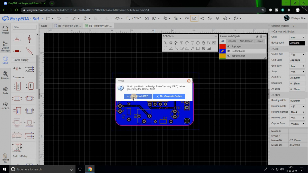
You will notice a window to check the routes. If you click on “yes,” the software will show you routing errors. Be aware that if you used flags or ports to name a pin and later made the connections, it will show those connections as an error.
Once you are sure the connections are correct, move to the next step. You will see a pop-up window like below.
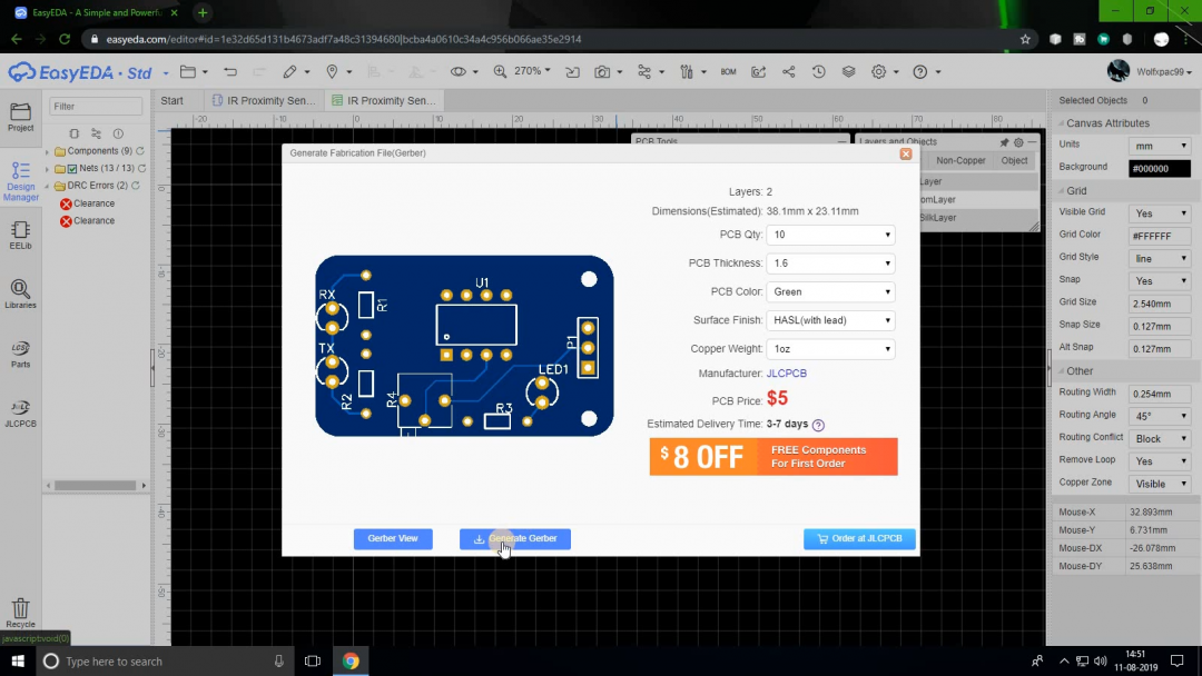
Here you can download the Gerber files and send them to any PCB manufacturer (Get $5 Free on PCBWay) or order them directly from OshPark or JLCPCB.
Final Note
This is a basic tutorial to get you started with PCB designing. Now you can start converting your breadboard prototypes into professional-looking PCBs.
If you have any questions, feel free to comment down below.