
One of the mysterious areas in robotics is how circuits and electronics are manufactured. Printed circuit boards, or PCBs, are used in sensors, microcontrollers, and computing devices. But, how exactly are they made? Manufacturing a custom PCB can be challenging (and frustrating) if you don’t have a process to follow.
In this guide, we will walk through the process of manufacturing a PCB. More specifically, we will use the L298N motor controller from the Official Learn Robotics Kit to give a real-world example of how a common component is designed, engineered, and manufactured.
The Steps to Manufacture a PCB
After this article, you will know how to draw circuit schematics, create PCB layouts, and generate files to manufacture a PCB. Furthermore, we will use this information to generate a Bill of Materials (BOM) that can be sent to the manufacturer for print and assembly.
This process can be replicated and reused no matter what type of circuit or PCB you want to create. The high-level steps to decompose a PCB part or create a new PCB from scratch are very similar.
Finally, if you already have a set of schematics or Gerber files ready for manufacturing, you can jump to the end and get started straight away.
What are PCBs?
PCB stands for printed circuit boards and is a set of conductive and layered boards used to affix electronic components.
PCBs are used for computing, sensing, and control and are found in common household electronics (not just robots).
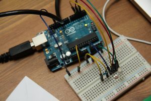
Once you have a circuit prototype finalized, you may want to move it from a breadboard (more temporary) to a permanent solution. A common option is to solder the components to a perf board or to generate schematics and layouts for a manufactured PCB.
How are PCBs made?
In this guide, we will explore the L298N motor controller from the Official Learn Robotics Kit to give you the process of making PCBs.
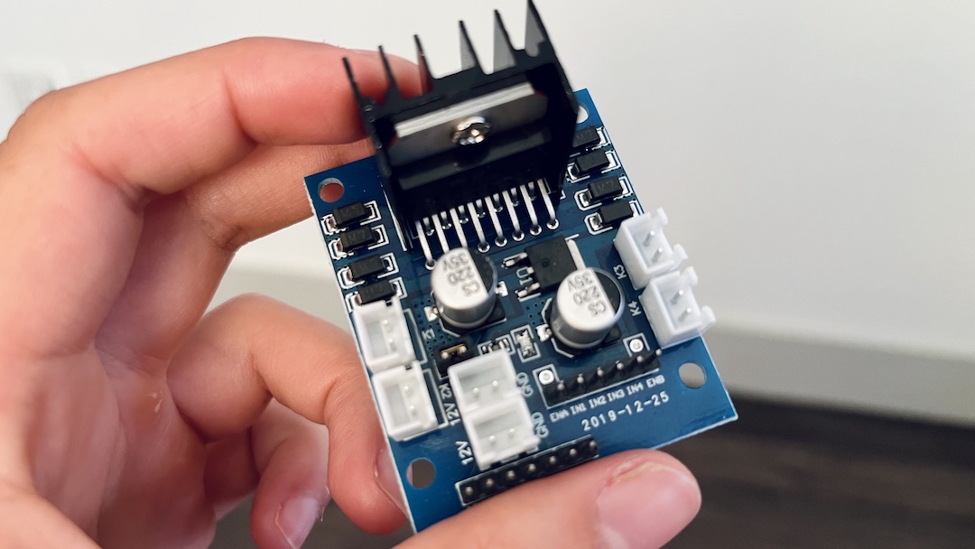
The L298N motor controller is a dual H-bridge that can control four DC motors. We use it to control speed and direction while ensuring there’s enough current for the motors. We will recreate the drawings for the L298N by designing schematics and a PCB layout. Then, we’ll generate a BOM and put together instructions for full PCB manufacturing and assembly.
Step 1: Understand PCB Hardware & Software Requirements
The first steps to creating a PCB are planning and designing. So before getting started, We first need to understand the hardware and software requirements for our board.
Here are the hardware requirements:
- A motor driver IC: We will use the motor controller driver to control 4 DC motors, so we need an Integrated Circuit or IC, that can withstand the load. For this, we have opted for the L298N dual motor driver as it is one of the most popular motor driver ICs in the market and has enough power to drive 4 DC motors (2 sets independently).
- Power supply: Our motor driver and other components require a stable 5V supply for which we will use a voltage regulator to convert 12V to 5V.
- Other components: These components will not work on their own. They need other active and passive components that will be added as we progress through the circuit design.
The next step is understanding the components we are using. If you’re building a PCB using familiar or off-the-shelf components, you’ll want to refer to the datasheet.
In our example, we are using the L298N in the Learn Robotics Kit, so we can pull its datasheet to understand how it functions and what additional components it requires to work.
After referring to the datasheet and understanding our components, we can move on to the software requirements. The software we are using here is called EasyEDA. EasyEDA is a free online tool to create circuits and design PCBs.
Step 2: Pick a Software to Design PCB Files
It doesn’t really matter which software you use to design circuits and PCB layouts. A few popular ones are KiCAD and Eagle. I opted to use EasyEDA because of its simplicity and vast source of libraries.
Let’s take a look at the EasyEDA User Interface.
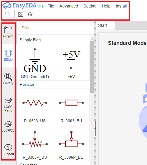
At the top, we can see a menu. This is the main menu of the software. Here we can access the files, import/export files, and create new designs/layouts/projects. We can also manage the settings of the app from here.
Next, on the left side, we have a components menu. Here we can find the project list and list of components we need for building schematics.
Now, let’s start with the process of designing a circuit.
Part A: Design the Circuit Schematics
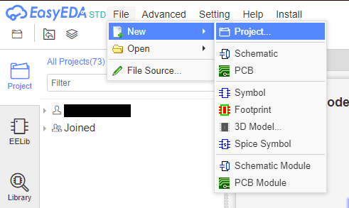
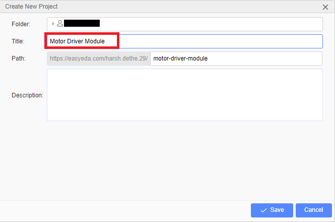
First, make a new project. Go to Files > Project.
In the new window, fill in the details like Project name and description.
Then, we named our project “Motor Driver Module,” since that’s what we’re making. The description is optional.
Next, we’ll see a blank canvas as shown in the image below. There are five major sections.
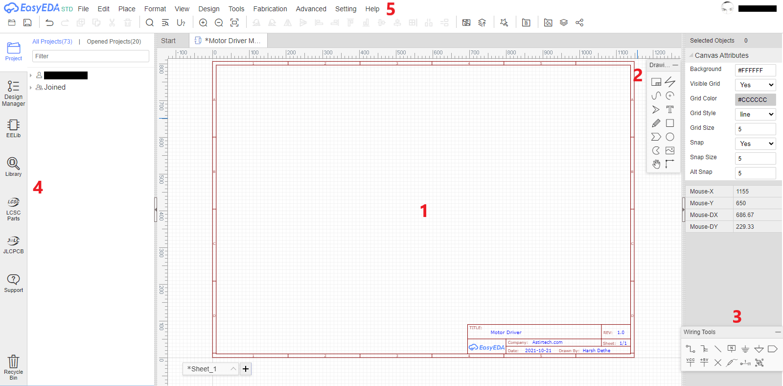
- Canvas: Here we create the circuit diagram.
- Drawing Tools: This contains all the tools necessary to create the drawing (labels, shapes, adding images).
- Wiring Tools: Contains all the tools required for wiring, making connections, and pins.
- Navigation List: Here we have options to find pre-built components for our designs.
- Toolbar: The toolbar contains the necessary features for setting design rules, Fabrication options, and viewing tools.
Add Components to the Drawing
Now we start building the schematic diagram by adding all the components we need for our circuit. First, look at the L298N datasheet and then select the component from the library.
Click on “Library” and search for the name of the component in the search bar.
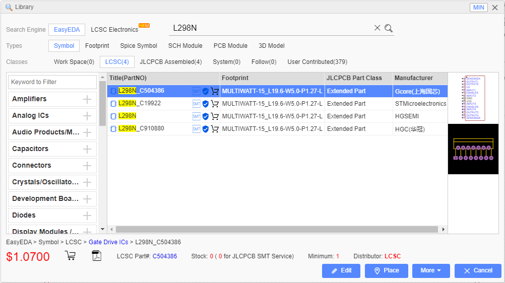
As in the image above we have searched for L298N and selected the one from the list that has footprints.
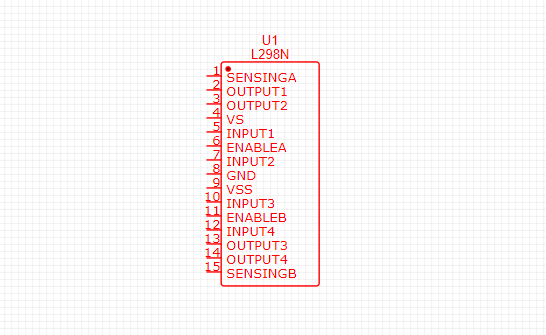
Then, double-click the component to add it to the canvas. This is what it will look like.
Similarly, refer to the datasheet to import all of the required components onto the canvas. Some of the components we added are diodes, capacitors, resistors, and a linear regulator.
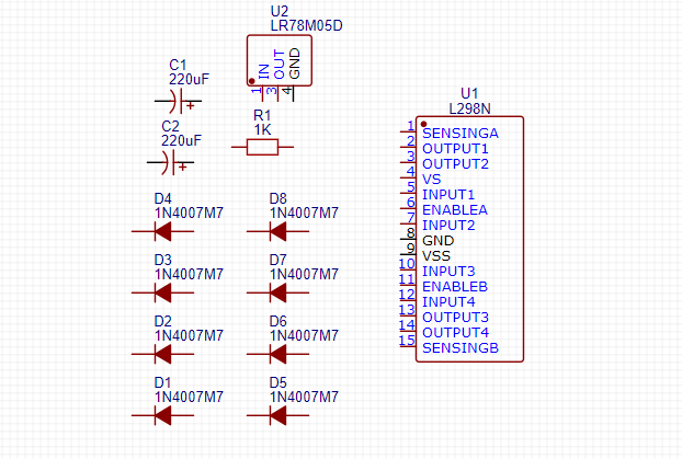
After all of the components are imported, arrange them according to the way they need to be connected. I organized the components into categories (Power, Input, Controller, Output).
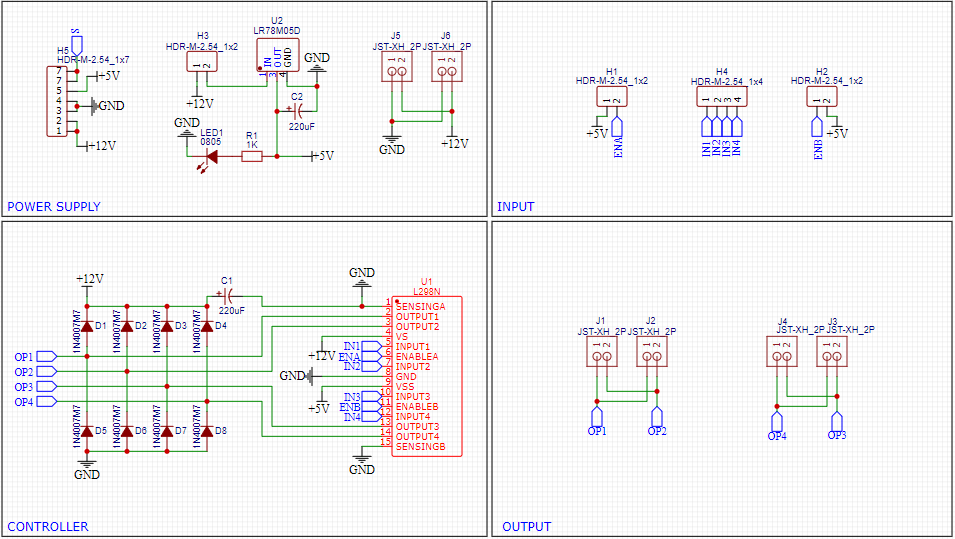
Let’s look at each category in detail:
- Power Supply: Here we have used a 7805 voltage regulator IC. It takes 12V input and provides a stable 5V for powering all electronics.
- Controller: This is the main motor driver IC L298N.
- Input: These are the input pins that will be connected to a microcontroller and receive commands.
- Output: We connect the motors here.
You can see the four categories arranged in separate boxes to make the schematic more readable. This helps a lot in the future to upgrade the circuit if needed.
After we have a schematic diagram, it’s time to make the PCB layout.
Part B: Create the PCB Layout
The PCB layout is how the PCB will look. It organizes the components and connections from the schematic to a design that represents the manufactured board.
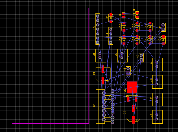
To turn the Schematic into a PCB layout, click on Design > Convert to PCB. This will take us to a new tab with all the components now turned into footprints.
Next, we’ll set the size of the PCB using an outline.
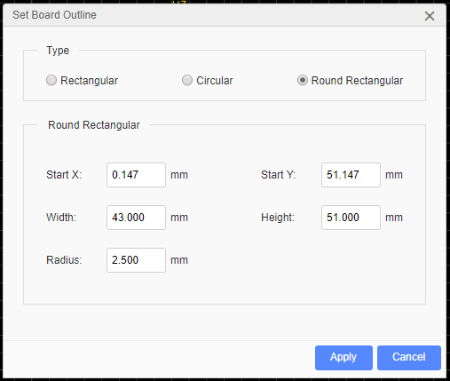
Go to Tools > Set Board Outline.
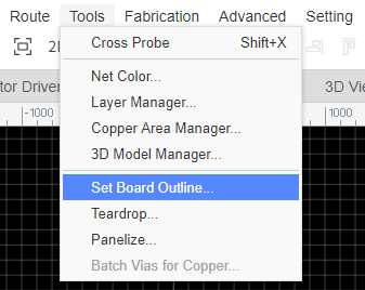
On the next pop-up window, fill out the dimensions of the board. Refer to the image below:
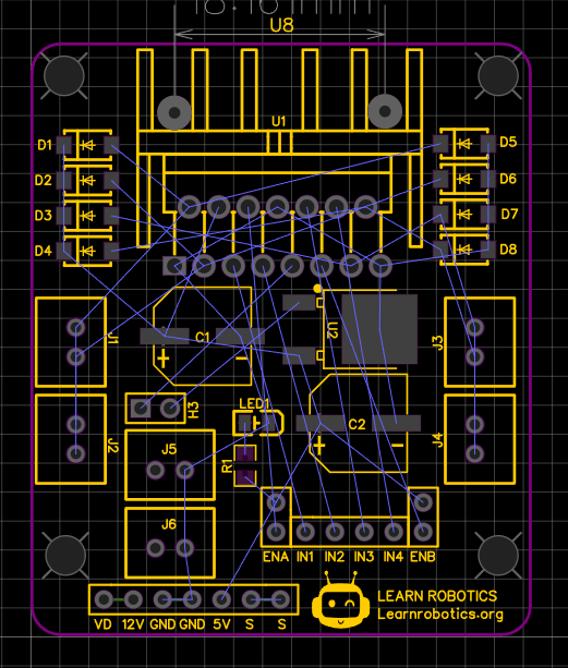
After setting the outline, it’s time to arrange the components on the board. This may take some time because we have to make sure everything fits and connects properly.
You can see how I placed the components to make all the ports accessible, below.
Once you complete the layout, it’s time to create the traces.
Part C: How to Setup Traces for PCBs
First, use the schematic to make sure everything is connected properly. You can use the nets feature to show how connections can be made, but sometimes this is unreliable.
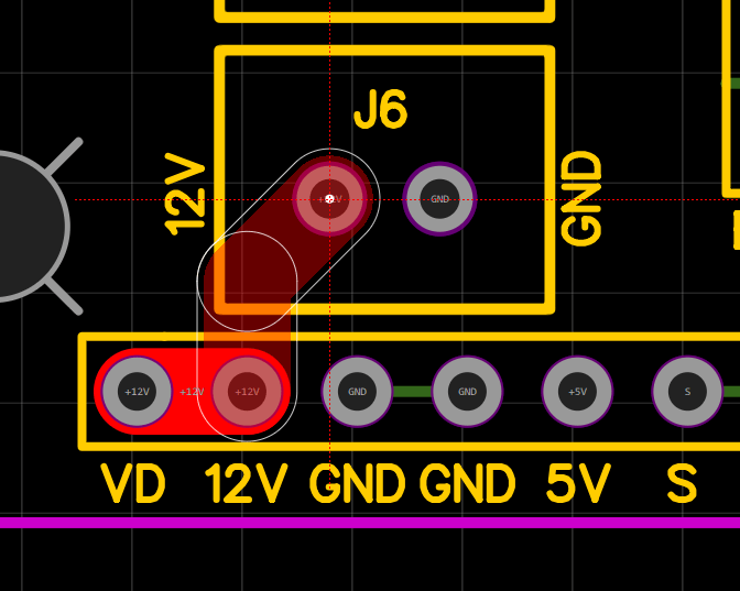
The traces that are going to carry 12V and drive the motors will be under more current, hence we make them thicker. Other traces can be lower than 0.5mm.
Below is the image of the final result after making all the connections.
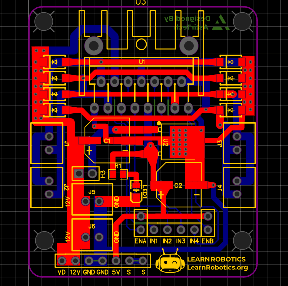
You can see that I have made a two-layer PCB, the RED traces go on top and the Blue ones go on the bottom. Make the connections between the top and bottom layers using vias. Now we can move on to check a 3D render of this design, before making the final Gerber.
Part D: Check the Design Before Generating the Final Gerber File
Next, click on the 3D option on the top toolbar to see the 3D view of the board.
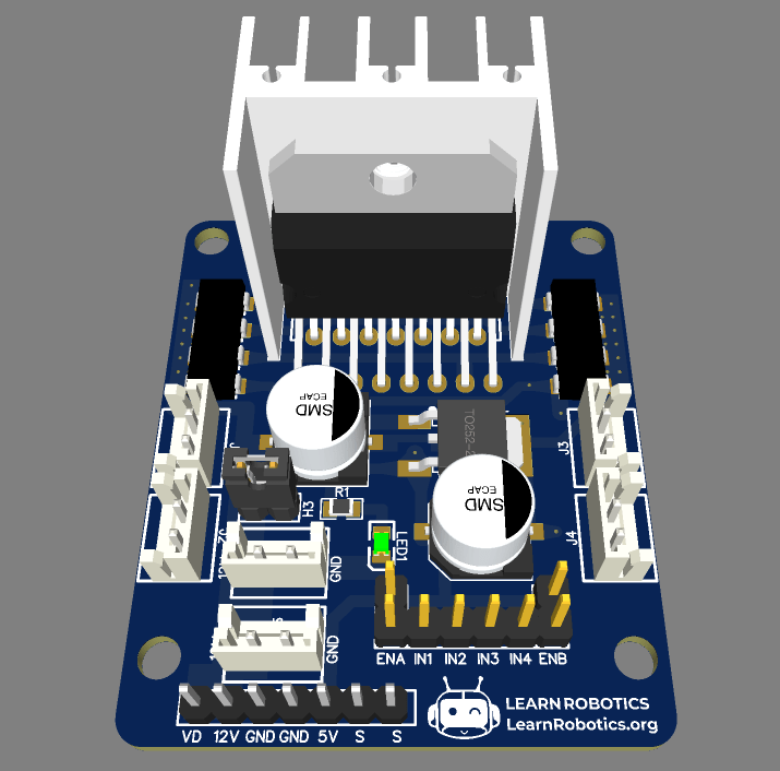
Then, a new tab will open and we can see the 3D model of our PCB. Here’s what the L298N motor controller looks like.
Once we have the design files, it’s time to make the fabrication files.
Step 3: Create Fabrication Files to Manufacture a PCB
Next, we will create the fabrication files for manufacturing. They consist of the following drawings:
- Gerber Files: a collection of files that define the PCB layers, outlines, drill patterns, and assembly information
- Bill of Materials (BOM): the parts and quantities needed to assemble the PCB
- Pick and Place File: Footprint and coordinates about how to assemble the PCB when using a manufacturing service.
- Schematic: The circuit wiring diagram for your circuit part
- PCB Info: General Specifications about the PCB
Generating files in EasyEDA is easy! In the next sections, we’ll walk through how to generate each file and what the file is used for.
Gerber Files
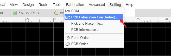
When you finish drawing your PCB, generate the Gerber Files by going to File > Generate PCB Fabrication File(Gerber). In the popup window, choose “Generate Gerber.”
Bill of Materials (BOM)
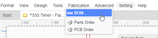
Whether you choose to assemble the PCB yourself or have it manufactured, you’ll want a copy of the BOM. This file will give you a list of parts and their quantities. You can export the Bill of Materials (BOM) for the schematic (Document) and PCB, by going to File > Export BOM. In the popup window, choose “Export BOM” on the bottom.
Pick and Place File
If you’re having a manufacturing service assemble your PCB, you’ll need to provide them with a Pick and Place file. This file provides the footprint and coordinates to assemble your PCB correctly.
To generate the Pick and Place File, go to File > Export Pick and Place File.
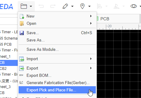
In the popup window, you’ll be able to choose from “mirrored coordinates’ and “include panelized components” in the pick and place file. Your best bet is to check with the PCB manufacturer to see which option works best with their process.
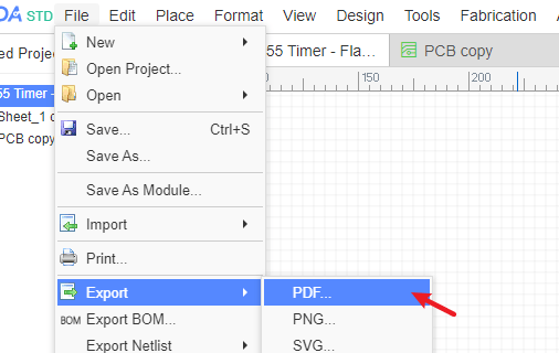
Schematic
It’s a good idea to create a PDF version of your schematic for reference. Generate a schematic for your part by going to File > Export > PDF. You can also save the schematic as other file types depending on your needs.
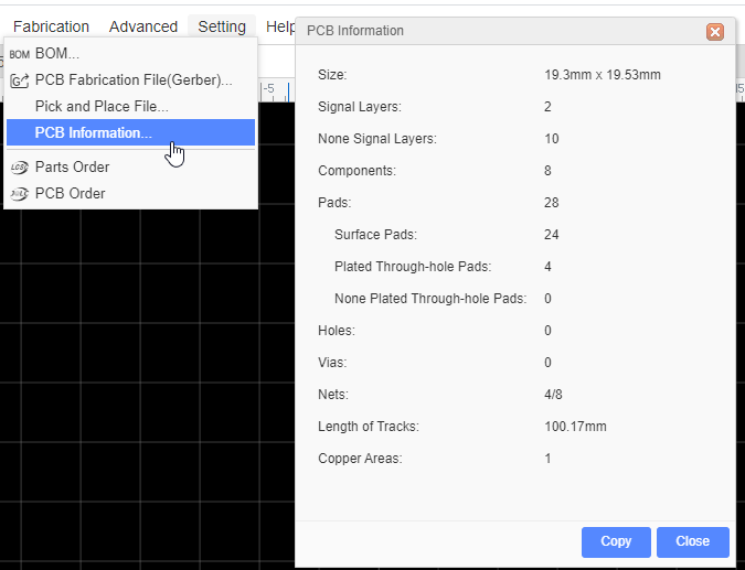
PCB Info
This is optional, but necessary if you want to have your PCBs manufactured. Get the PCB Info by going to the Top Menu > Fabrication > PCB Information. Then, press the “Copy” button. Open a spreadsheet and paste this information for easy access.
Step 4: How to Use Fabrication Files and Schematics to Manufacture a PCB
Once you have your fabrication files, it’s time to manufacture a PCB. We teamed up with NextPCB for this article to show you the process of ordering PCBs.
NextPCB was founded in 2004 and has since established itself as a turnkey PCB manufacturing and assembly factory for prototyping quantities as well as small-volume to large-scale production.
NextPCB provides a one-stop shop for PCB design and manufacturing with professional practices for filling advanced requirements for even the most complex circuits. Their company provides rapid solutions for PCBs and assembly of PCBs and components. NextPCB uses quality assurance practices to ensure that your boards are manufactured with the correct specs and arrive ready to use!
If you’re looking for a manufacturer to take on your next batch of PCBs—both printing and assembly—check out NextPCB.com. You can use the Learn Robotics link to get 10 free PCBs and free shipping!
Now, let’s walk through the steps to manufacture PCBs and PCB assembly services.
Part A: Upload the Gerber Files (.zip) folder
First, upload the Gerber files (.zip) folder to NextPCB uploader. You’ll see a preview of the board. Double-check that this looks like the board you designed before moving on.
Part B: Choose Your PCB Settings
Then, choose your PCB settings. The default settings are usually pretty good. Make sure you choose the quantity and number of layers for your PCB. Also, double-check that the PCB dimensions are correct.
Part C: Add Turnkey PCB Assembly (Optional)
Next, you can choose to add Turnkey PCB Assembly. If you choose this option, NextPCB will source the components in the circuit BOM, place them, and assemble the PCBs.
This is a great option if you have a complex circuit and want to ensure that assembly is high quality.
To add turnkey PCB assembly, you’ll need to use the PCB Info from EasyEDA. This can be accessed in Top Menu > Fabrication > PCB Information. I copied this into a Spreadsheet for easy access.
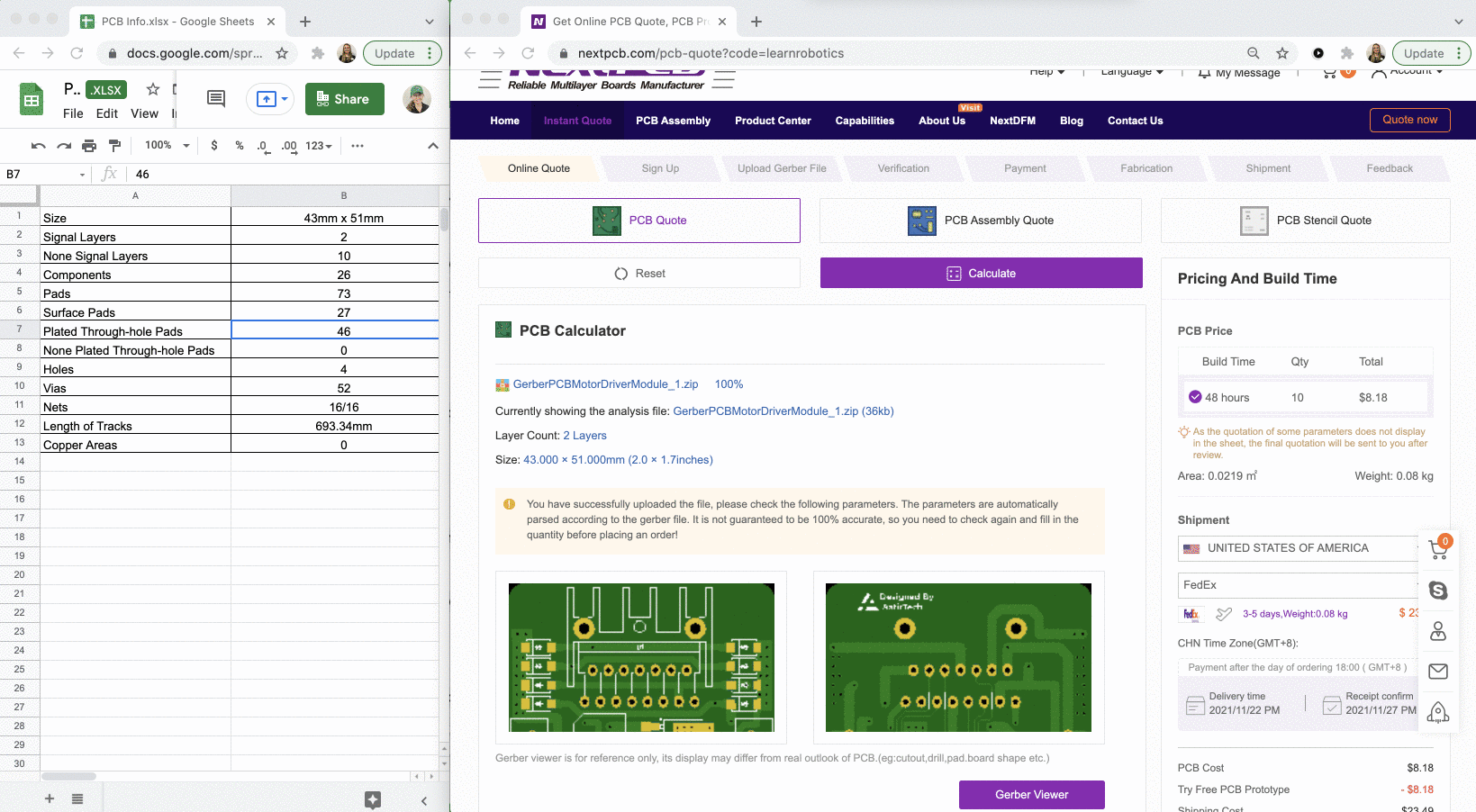
You’ll want to type in the quantity of PCBs that need assembly (typically the same quantity of PCBs that you’re purchasing). Then, you’ll type in how many components, pads, and through-hole pads from the PCB info into the NextPCB ordering form.
Lastly, double-check your PCB dimensions and choose whether you want the PCBs to be packaged in Anti-Static (ESD) bags or not.
Once you’re happy with the settings, click “Add to Cart”.
Part D: Complete the Purchase
Finally, complete the purchase.
You’ll need to log in or create an account if you don’t have one. Make sure you add any requested files (such as Parts List, BOM, Pick and Place, etc.).
NextPCBs system will request the files that it needs to complete your order. Enter your billing and shipping info, and complete the order. You’ll receive an estimated completion and ship date.
And voilà! The hard work is done! Now it’s just waiting for the PCBs to arrive!
Manufacture a PCB and Post-Production Process
For this project, we chose to have our PCBs ordered, assembled, and packed in an ESD bag by NextPCB. You can choose the right settings for the board you’re trying to make. If it’s something simple, you may choose to assemble and solder the components yourself. However, for complex assemblies, it might be worth paying for the turnkey assembly option. You’ll save a bunch of time and have the quality assurance that you just can’t match in a DIY setting.
Once the L298N PCBs arrive at our Studio HQ, they go into the kitting queue where our team packs and assembles the Level 1 & 2 Kits for the Specialist Certification training.
I think it’s important as an engineering professional to showcase a living, breathing application of how to manufacture a PCB from ideation to production. That’s why we chose the L298N board from our Level 2 kit as a case study — you can see a tangible instance of PCB manufacturing in a product that is readily accessible (and useful) for robotics!
Plus, the next time you enroll in a Learn Robotics training or pick up a kit, you’ll have the chance to get one of the 10 boards from this production run! And, even if you don’t walk away with one of the golden boards, you’ll have the tools behind the engineering process for just about any PCB you decide to create!